| CPC H01L 23/49838 (2013.01) [H01L 21/486 (2013.01); H01L 21/4857 (2013.01); H01L 23/49822 (2013.01); H01L 23/49827 (2013.01); H05K 1/111 (2013.01); H05K 1/115 (2013.01); H05K 1/025 (2013.01); H05K 1/18 (2013.01); H05K 2201/095 (2013.01); H05K 2201/09727 (2013.01); H05K 2201/09736 (2013.01); H05K 2201/09827 (2013.01)] | 8 Claims |
|
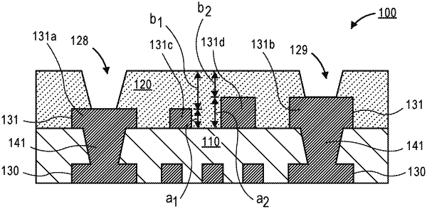
1. A package substrate, comprising:
a conductive layer in a dielectric;
a first trace and a first via pad of the conductive layer having a first thickness, the first via pad having an uppermost surface;
a second trace and a second via pad of the conductive layer having a second thickness, wherein the second thickness of the second trace and the second via pad is greater than the first thickness of the first trace and the first via pad, and the second via pad having an uppermost surface above the uppermost surface of the first via pad, and wherein the dielectric includes a first via opening exposing the uppermost surface of the first via pad, and the dielectric includes a second via opening exposing the uppermost surface of the second via pad, the first via opening extending a depth in the dielectric greater than a depth of the second via opening.
|