| CPC H01L 21/76816 (2013.01) [H01L 21/31144 (2013.01)] | 10 Claims |
|
1. A method for forming a semiconductor device, comprising:
providing a to-be-etched layer including a first region and a second region adjoining the first region;
forming a first mask layer on the to-be-etched layer;
forming a patterned core layer on the first mask layer of the first region;
forming a sidewall spacer on a top surface and a sidewall surface of the core layer and a surface of the first mask layer;
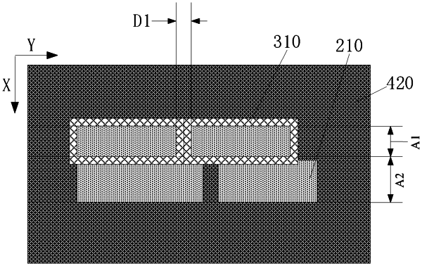
forming a first sacrificial layer on the sidewall spacer on the surface of the first mask layer of the second region, a top surface of the entire first sacrificial layer being higher than the top surface of the core layer, forming the first sacrificial layer including:
forming a first sacrificial material layer on a top surface and sidewall surfaces of the sidewall spacer;
forming a patterned photoresist layer on a top surface of the first sacrificial material layer, the patterned photoresist layer covering the first sacrificial material layer of the second region; and
using the patterned photoresist layer as a mask to etch the first sacrificial material layer to form the first sacrificial layer on the sidewall spacer on the surface of the first mask layer of the second region;
forming a second sacrificial layer on the sidewall spacer, the second sacrificial layer exposing the sidewall spacer on the top of the core layer and a top of the first sacrificial layer;
removing the entire first sacrificial layer, the sidewall spacer on the surface of the first mask layer of the second region and the sidewall spacer on the top of the core layer;
removing the core layer after the entire first sacrificial layer is removed;
etching the first mask layer of the first region to form a first trench; and
etching the first mask layer of the second region to form a second trench.
|