| CPC H01L 21/31144 (2013.01) [H01L 21/76816 (2013.01); H01L 21/31155 (2013.01)] | 18 Claims |
|
1. A forming method of a semiconductor structure, comprising:
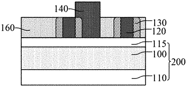
providing a base, comprising a target layer configured to form a target pattern;
forming mandrel lines that extend along a first direction and are arranged at intervals along a second direction on the base, wherein the second direction is perpendicular to the first direction, and wherein opposite sidewalls of adjacent mandrel lines in the second direction are a first sidewall and a second sidewall;
forming a sacrificial spacer on a sidewall of the mandrel line;
after forming the sacrificial spacer, forming a sacrificial layer extending along the first direction on a part of the base between adjacent sacrificial spacers, wherein the sacrificial layer covers a sidewall of a sacrificial spacer located on the first sidewall, and is spaced apart from a sacrificial spacer located on the second sidewall;
forming a filling layer on the base exposed by the mandrel line, the sacrificial spacer, and the sacrificial layer;
removing the sacrificial layer, to form an opening in the filling layer;
removing the sacrificial spacer, wherein the opening and the first sidewall form a trench;
forming a mask spacer on a sidewall of the trench, wherein the mask spacer is further filled between the sidewall of the mandrel line and the filling layer, and the mask spacer located on the sidewall of the trench forms a first groove;
forming a second groove running through the filling layer between the sidewall of the trench and the mask spacer located on the second sidewall;
performing ion doping on a part of the mandrel line to increase etching resistance of the mandrel line, and using the part of mandrel line doped with ions as a third cutting layer cutting the mandrel line along the first direction;
removing the mandrel line, to form a third groove, wherein a cutting layer is formed in at least one of the third groove, the second groove, and the first groove, and the cutting layer cuts the corresponding groove along the first direction; and
patterning the target layer below the third groove, the second groove, and the first groove using the cutting layer, the mask spacer, and the filling layer as a mask, to form the target pattern.
|