US 11,769,537 B2
Memory device and memory system including the same
Byunghoon Jeong, Hwaseong-si (KR); Kyungtae Kang, Seoul (KR); Jangwoo Lee, Seoul (KR); and Jeongdon Ihm, Seongnam-si (KR)
Assigned to Samsung Electronics Co., Ltd., Gyeonggi-do (KR)
Filed by Samsung Electronics Co., Ltd., Suwon-si (KR)
Filed on Dec. 21, 2022, as Appl. No. 18/69,685.
Application 18/069,685 is a continuation of application No. 17/411,421, filed on Aug. 25, 2021, granted, now 11,562,780.
Application 17/411,421 is a continuation in part of application No. 17/001,941, filed on Aug. 25, 2020, granted, now 11,107,512, issued on Aug. 31, 2021.
Claims priority of application No. 10-2019-0123349 (KR), filed on Oct. 4, 2019.
Prior Publication US 2023/0127635 A1, Apr. 27, 2023
Int. Cl. G11C 7/22 (2006.01); G11C 7/10 (2006.01); H03K 19/173 (2006.01); G11C 8/18 (2006.01); G11C 29/42 (2006.01)
CPC G11C 7/222 (2013.01) [G11C 7/1057 (2013.01); G11C 7/1063 (2013.01); G11C 7/1084 (2013.01); G11C 8/18 (2013.01); G11C 29/42 (2013.01); H03K 19/1737 (2013.01)] 20 Claims
OG exemplary drawing
 
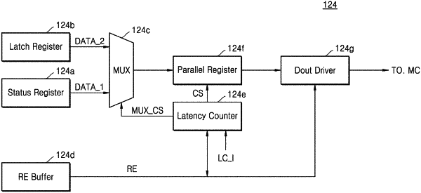
1. A memory device, comprising:
a memory cell array configured to store data; and
a data output circuit configured to transmit a data signal to an external device, wherein the data output circuit includes:
a latch register configured to store the data read from the memory cell array;
a status register configured to store status data; and
a multiplexer configured to select first output data of the status register during a latency period and second output data of the latch register during a period subsequent to the latency period.