| CPC G09G 3/3233 (2013.01) [G06V 40/1318 (2022.01); H10K 59/1213 (2023.02); H10K 59/1216 (2023.02); H10K 59/131 (2023.02); H10K 59/60 (2023.02); G09G 2310/0291 (2013.01)] | 8 Claims |
|
1. A pixel circuit sharing elements with a finger sensing circuit, the pixel circuit comprising:
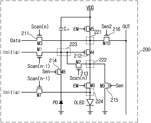
a driving transistor including a first terminal connected to a first node, a second terminal connected to a second node, and a gate terminal connected to a third node, the driving transistor configured to supply a driving current;
a sensing transistor including a first terminal directly connected to the first terminal of the driving transistor at the first node, and a second terminal connected to an output line of the pixel circuit;
a first transistor including a first terminal that is connected to a data line, a second terminal that is directly connected to the first terminal of the driving transistor at the first node and directly connected to the first terminal of the sensing transistor at the first node, and a gate terminal of the first transistor connected to a n-th scan line;
a self-light emitting element that displays images by emitting light responsive to the driving current controlled by a driving transistor, the self-light emitting element connected to the second node; and
a light-receiving element that receives the light emitted from the self-light emitting element and reflected through a fingerprint of a user and converts the light into an electrical signal, the light-receiving element connected to the gate terminal of the driving transistor at the third node;
wherein the pixel circuit reads, through the output line of the pixel circuit that is connected to the first terminal of the driving transistor at the first node while the sensing transistor is turned on, an output signal generated by the light-receiving element and output to the output line connected to the first terminal of the driving transistor via the driving transistor while the sensing transistor is turned on, and
wherein the pixel circuit converts the output signal received from the output line that is connected to the first terminal of the driving transistor while the sensing transistor is turned on from an analog signal into a digital signal, compares the digital signal with initial brightness data of the self-light emitting element prior to deterioration of the self-light emitting element over time, and compensates a voltage to be applied to the driving transistor based on a result of the comparison.
|