| CPC G09G 3/32 (2013.01) [G09G 2300/0842 (2013.01); G09G 2310/0267 (2013.01); G09G 2310/061 (2013.01); G09G 2320/0257 (2013.01)] | 12 Claims |
|
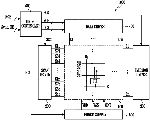
1. A pixel comprising:
a light emitting element;
a first node connected to a first driving power source;
a second node connected to an anode electrode of the light emitting element;
a first transistor connected between the first node and the second node and having a gate electrode connected to a third node;
a second transistor connected between a data line and the first node, the second transistor to be turned on by a first scan signal applied through a first scan line;
a third transistor connected between the second node and the third node, the third transistor to be turned on by a second scan signal applied through a second scan line;
a fourth transistor connected between the third node and a first initialization power source, the fourth transistor to be turned on by a third scan signal applied through a third scan line;
a first capacitor connected between the first driving power source and the third node; and
a second capacitor having an input electrode and an output electrode, and connected to the third node through the output electrode to boost a voltage of the gate electrode of the first transistor in response to change in a voltage of the input electrode.
|