| CPC G09G 3/32 (2013.01) [G09G 2300/0413 (2013.01); G09G 2300/0819 (2013.01); G09G 2300/0842 (2013.01); G09G 2310/061 (2013.01); G09G 2320/0233 (2013.01)] | 17 Claims |
|
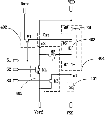
1. A display panel comprising a first area and a second area, comprising:
a plurality of first pixel rows, and each of the first pixel rows comprising a plurality of pixels;
a plurality of second pixel rows, and each of the second pixel rows comprising a plurality of pixels, wherein
the number of the pixels of each first pixel row is greater than the number of the pixels of each second pixel row; the plurality of pixels of the first pixel row are a plurality of display pixels, and the plurality of the pixels of the second pixel row are a plurality of display pixels and a plurality of virtual pixels;
each of the plurality of display pixels comprises a display pixel circuit, each of the plurality of virtual pixels comprises a virtual pixel circuit, the virtual pixel circuit comprises a compensation unit, and the virtual pixel circuit is configured to compensate the display pixel circuits of one of the plurality of second pixel rows when the display pixel circuits of the one of the plurality of second pixel rows are reset; so that, after the display pixel circuits in both the first area and the second area are reset, a voltage difference of nodes of light-emitting devices corresponding to the display pixel circuits is reduced;
wherein each of the display pixel circuit and the virtual pixel circuit comprises:
a writing unit, configured to receive a first scanning signal;
a driving unit, wherein the driving unit is connected to the writing unit by a driving node, and the writing unit is driven by the first scanning signal to write a data signal to the driving node in a writing stage;
a control unit, configured to receive an enable signal, wherein the control unit is connected to the driving unit, so that the driving unit is connected to a power signal line by the control unit; and
a reset unit, configured to receive a second scanning signal, wherein the reset unit is connected to the driving node and the control unit, the reset unit is driven by the second scanning signal to receive a reference signal, and the reset unit resets the driving node and a first node which is between the reset unit and the control unit according to the reference signal; and
wherein one end of the compensation unit is connected to the driving node, and the other end of the compensation unit is connected to the power signal line.
|