| CPC G06F 3/0443 (2019.05) [G06F 3/0446 (2019.05); H10K 59/40 (2023.02); G02B 5/3025 (2013.01)] | 27 Claims |
|
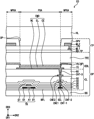
1. An electronic device including an active area and a peripheral area disposed adjacent to the active area, the electronic device comprising:
a display layer;
a sensor layer disposed on the display layer; and
a high refraction layer disposed on the sensor layer, wherein
the sensor layer comprises:
a first conductive layer;
a second conductive layer disposed on the first conductive layer;
an inorganic insulation layer disposed between the first conductive layer and the second conductive layer; and
an organic insulation layer disposed between the second conductive layer and the high refraction layer,
in the peripheral area, at least one opening is defined in the organic insulation layer, and
in the at least one opening of the organic insulation layer, the inorganic insulation layer does not overlap the organic insulation layer and the second conductive layer.
|