| CPC G03F 7/70625 (2013.01) [G06F 30/20 (2020.01); G06T 7/0004 (2013.01); H01L 22/20 (2013.01); G03F 1/00 (2013.01); G06F 30/33 (2020.01); G06F 30/398 (2020.01); G06F 2119/18 (2020.01); G21K 5/00 (2013.01); H01L 21/00 (2013.01)] | 20 Claims |
|
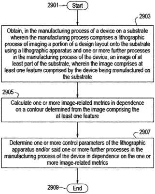
1. A method for a manufacturing process of a device on a substrate, wherein the manufacturing process comprises a lithographic process of imaging a portion of a design layout onto the substrate using a lithographic apparatus and one or more further processes in the manufacturing process of the device, the method comprising:
obtaining an image of at least part of the substrate, wherein the image comprises at least one feature comprised by the device being manufactured in a layer on the substrate;
obtaining a layout of features associated with a previous layer adjacent to the layer on the substrate;
calculating one or more image-related metrics in dependence on: 1) a contour determined from the image comprising the at least one feature and 2) the layout of features; and
determining one or more control parameters of the lithographic apparatus and/or the one or more further processes in the manufacturing process of the device in dependence on the one or more image-related metrics, wherein at least one of the one or more control parameters is determined to modify the geometry of the contour in order to improve the one or more image-related metrics.
|