| CPC G02F 1/136286 (2013.01) [G02F 1/1368 (2013.01)] | 12 Claims |

|
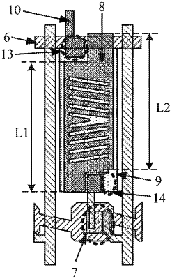
1. A display substrate, comprising: a first base substrate, and a plurality of gate lines and a plurality of data lines which are positioned on the first base substrate, wherein the gate lines extend along a first direction, the data lines extend along a second direction, and the first direction and the second direction are crossed and are parallel to a plane where the first base substrate is positioned;
the plurality of gate lines and the plurality of data lines define a plurality of pixel units, and each of the pixel units comprises a thin film transistor, a pixel electrode and a common electrode, the pixel electrode is positioned on a side of the common electrode away from the first base substrate, an area where the pixel electrode is positioned and an area where the thin film transistor is positioned in a same one of the pixel units are arranged along the second direction, an end, proximal to the thin film transistor, of the pixel electrode is a first end part, an end, away from the thin film transistor, of the pixel electrode is a second end part, at least a portion of the pixel units are provided with a conductive bridge line, and the conductive bridge line and the pixel electrode are arranged in a same layer;
in the pixel unit configured with the conductive bridge line, the pixel electrode has a first notch on a first side of the first end part or the second end part of the pixel electrode, an end of the conductive bridge line is located in the first notch and is coupled to the common electrode through a via hole, and the pixel electrode has a second notch on a second side of at least one of the first end part or the second end part of the pixel electrode, so that lengths of a first portion and a second portion of the pixel electrode, that generate lateral capacitances respectively with the data lines located on two sides of the pixel electrode and closest to the pixel electrode, in the second direction, are substantially equal to each other, and an absolute value of a difference between the lateral capacitances respectively formed between the pixel electrode and the data lines which are located on the two sides of the pixel electrode and are closest to the pixel electrode is less than or equal to a preset capacitance difference value;
the first side and the second side are opposite sides of the pixel electrode in the first direction.
|