| CPC G02F 1/1345 (2013.01) [G02F 1/1334 (2013.01); G02F 1/1337 (2013.01); G02F 1/1339 (2013.01); G02F 1/133512 (2013.01); G02F 1/134309 (2013.01); G02F 1/136286 (2013.01)] | 7 Claims |
|
1. A display device comprising:
an array substrate comprising a plurality of pixel electrodes;
a counter substrate comprising a common electrode in a position at least overlapping the pixel electrodes;
a liquid crystal layer between the array substrate and the counter substrate; and
a light source disposed so as to emit light into a side surface of the array substrate or a side surface of the counter substrate, wherein
the array substrate comprises, in a display region:
a plurality of signal lines arranged in a first direction with spaces between the signal lines;
a plurality of scanning lines arranged in a second direction with spaces between the scanning lines; and
common potential wiring provided outside the display region,
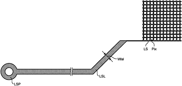
the counter substrate comprises light-blocking coupling wiring that couples the common electrode to a first power feeding portion, which is an annular body,
the common potential wiring has a mesh shape, and
the array substrate comprises a second power feeding portion having a metal layer filling the meshes of the common potential wiring in a position overlapping an opening of the annular body of the first power feeding portion.
|