| CPC G02B 6/4214 (2013.01) [G02B 6/12002 (2013.01); G02B 6/12004 (2013.01); G02B 6/136 (2013.01); G02B 6/4203 (2013.01); G02B 6/4204 (2013.01); G02B 6/43 (2013.01); G02B 6/428 (2013.01); G02B 2006/12102 (2013.01); G02B 2006/12104 (2013.01)] | 20 Claims |
|
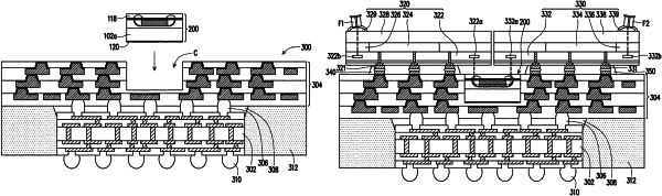
5. A structure, comprising:
a circuit substrate;
an insulating encapsulation laterally encapsulating the circuit substrate;
a redistribution circuit structure disposed on the circuit substrate and the insulating encapsulation, wherein the redistribution circuit structure comprises a cavity; and
an optical interconnect structure placing in the cavity, comprising:
a base substrate, comprising:
a semiconductor substrate; and
a base dielectric layer disposed on a first surface of the semiconductor substrate;
an optical waveguide embedded in the base substrate, the optical waveguide comprising a first end portion, a second end portion opposite to the first end portion, and a guiding portion embedded in the base substrate, and the guiding portion is between the first end portion and the second end portion, and wherein an interface is formed between the guiding portion and the first end portion;
a first reflector disposed between the base substrate and the first end portion of the optical waveguide, wherein the first reflector is spaced apart from the guiding portion by the first end portion;
a second reflector disposed between the base substrate and the second end portion of the optical waveguide;
a dielectric layer covering the base substrate and the optical waveguide;
a first lens disposed on the dielectric layer and located above the first end portion of the optical waveguide;
a second lens disposed on the dielectric layer and located above the second end portion of the optical waveguide; and
an adhesive layer disposed on a second surface of the semiconductor substrate, wherein the second surface is opposite to the first surface,
wherein the optical interconnect structure is adhered to a bottom surface of the cavity through the adhesive layer.
|