| CPC C09K 11/883 (2013.01) [C09K 11/02 (2013.01); C09K 11/565 (2013.01); B82Y 20/00 (2013.01); B82Y 40/00 (2013.01); H10K 50/115 (2023.02); Y10S 977/774 (2013.01); Y10S 977/824 (2013.01); Y10S 977/892 (2013.01); Y10S 977/95 (2013.01)] | 19 Claims |

|
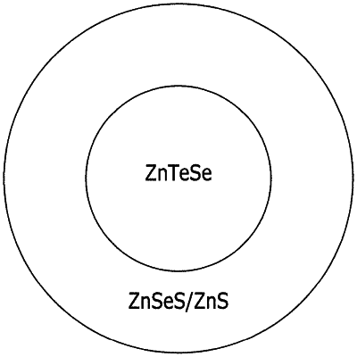
1. A semiconductor nanocrystal particle comprising
zinc,
tellurium, and
selenium,
wherein a mole ratio of the tellurium to the selenium is less than 0.01:1,
wherein the semiconductor nanocrystal particle emits blue light comprising a maximum peak emission at a wavelength of greater than or equal to 449 nanometers (nm) and less than or equal to about 470 nanometers (nm), and
wherein the maximum peak emission has a full width at half maximum of less than or equal to about 40 nm or wherein the semiconductor nanocrystal particle is configured to show a quantum efficiency of greater than or equal to about 60%.
|