| CPC H10N 50/01 (2023.02) [G11C 11/161 (2013.01); H01L 29/82 (2013.01); H10N 50/10 (2023.02); H10N 50/80 (2023.02); H10N 50/85 (2023.02)] | 14 Claims |

|
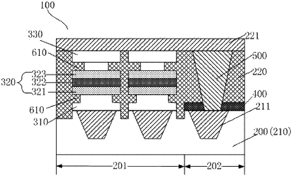
1. A semiconductor structure, comprising:
a base substrate;
a bottom electrode layer on the base substrate;
a magnetic tunnel junction layer on the bottom electrode layer; and
a top electrode layer on the magnetic tunnel junction layer, wherein openings are formed at least exposing a portion of an upper surface of the magnetic tunnel junction layer or a portion of a lower surface of the magnetic tunnel junction layer;
wherein:
the top electrode layer includes a first top electrode portion and a second top electrode portion, the second top electrode portion being located between the first top electrode portion and the magnetic tunnel junction layer, a maximum length of the first top electrode portion in a horizontal direction parallel to a top surface of the base substrate being same as a maximum length of the magnetic tunnel junction layer in the horizontal direction, and a maximum length of the second top electrode portion in the horizontal direction being smaller than the maximum length of the magnetic tunnel junction layer in the horizontal direction;
the openings include a first type opening or a second type opening;
the first type opening extends from a sidewall of the top electrode layer or a sidewall of the bottom electrode layer to a middle of the top electrode layer or a middle of the bottom electrode layer along a direction in parallel with the top surface of the base substrate;
the second type opening passes through the top electrode layer or the bottom electrode layer along a direction perpendicular to the top surface of the base substrate; and
the openings expose the portion of the upper surface of the magnetic tunnel junction layer and the portion of the lower surface of the magnetic tunnel junction layer.
|