| CPC H10K 50/84 (2023.02) [G06F 3/041 (2013.01); G06F 2203/04107 (2013.01); H01L 25/167 (2013.01); H10K 59/12 (2023.02)] | 11 Claims |

|
1. A display apparatus comprising:
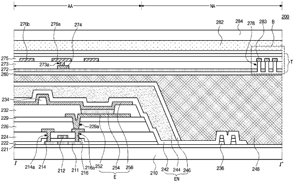
a substrate including a display area and a non-display area;
a thin film transistor in the display area;
a first passivation layer over the thin film transistor;
a planarization layer on the first passivation layer;
a light emitting device on the first passivation layer, the light emitting device including a first electrode, a light emitting layer on the first electrode, and a second electrode on the light emitting layer;
at least one dam in the non-display area;
an encapsulation layer covering the light emitting device, the encapsulation layer including a first encapsulation layer made of an inorganic material, a second encapsulation layer made of an organic material on the first encapsulation layer, and a third encapsulation layer made of an inorganic material on the second encapsulation layer;
an adhesive over the encapsulation layer;
a touch sensor on the adhesive, the touch sensor including a buffer layer on the adhesive, a bridge on the buffer layer, an interlayer insulating layer on the bridge, a first touch electrode and a second touch electrode on the interlayer insulating layer, and a second passivation layer over the first touch electrode and the second touch electrode;
at least one crack propagation blocking member formed in the buffer layer and the interlayer insulating layer; and
a gas blocking member formed on the interlayer insulating layer to cover the at least one crack propagation blocking member;
wherein the first encapsulation layer and the third encapsulation layer extend to the non-display area and cover the at least one dam, and
wherein a side surface of the encapsulation layer is slanted in the non-display area and the adhesive is formed in the slanted side surface of the encapsulation layer.
|