| CPC H10B 41/27 (2023.02) [H10B 41/10 (2023.02); H10B 43/10 (2023.02); H10B 43/27 (2023.02); H10B 51/10 (2023.02); H10B 51/20 (2023.02)] | 20 Claims |

|
1. A method for manufacturing a semiconductor memory device, comprising:
forming a stack structure on a substrate, the stack structure including a plurality of dielectric layers and a plurality of sacrificial layers alternatingly stacked in a Z direction perpendicular to the substrate;
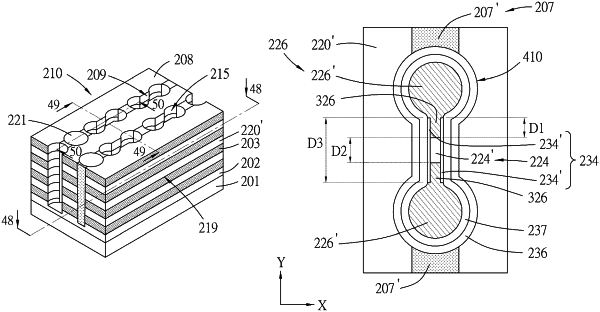
forming a plurality of first isolation trenches each penetrating the stack structure in the Z direction, and at least one second isolation trench penetrating the stack structure in the Z direction, the plurality of first isolation trenches and the at least one second isolation trench being aligned in a Y direction parallel to the substrate, the at least one second isolation trench having a length in the Y direction greater than a length of each of the plurality of first isolation trenches in the Y direction;
forming a plurality of dielectric isolation segments respectively filling the plurality of first isolation trenches and the at least one second isolation trench;
forming a plurality of channel trenches, each of the plurality of channel trenches penetrating the stack structure in the Z direction and being disposed between two adjacent ones of the plurality of dielectric isolation segments;
forming a plurality of first sacrificial segments respectively filling the plurality of channel trenches;
forming a plurality of source/drain trenches each extending in the Z direction and penetrating the stack structure, a corresponding one of the plurality of dielectric isolation segments and a corresponding one of the plurality of first sacrificial segments, the plurality of source/drain trenches, the plurality of dielectric isolation segments and the plurality of first sacrificial segments being aligned in the Y direction;
forming a plurality of second sacrificial segments respectively filling the plurality of source/drain trenches;
forming at least one through hole extending in the Z direction and penetrating the stack structure and an immediately adjacent one of the plurality of dielectric isolation segments;
removing the plurality of sacrificial layers to form a plurality of spaces, the plurality of dielectric layers and the plurality of spaces being alternatingly disposed in the Z direction, the plurality of spaces being spatially communicated with the at least one through hole;
forming a plurality of conductive layers respectively filling the plurality of spaces;
forming at least one refill segment filling the at least one through hole;
removing the plurality of first sacrificial segments and the plurality of second sacrificial segments;
forming a memory layer in the plurality of channel trenches and the plurality of source/drain trenches;
forming a conductive channel layer on the memory layer;
forming a dielectric separation feature completely filling the plurality of channel trenches and partially filling the plurality of source/drain trenches;
removing the dielectric separation feature in the plurality of source/drain trenches to respectively form a plurality of dielectric separation segments in the plurality of channel trenches; and
forming a conductive feature filling the plurality of source/drain trenches.
|