| CPC H10B 10/125 (2023.02) [H01L 21/0259 (2013.01); H01L 21/28518 (2013.01); H01L 21/823807 (2013.01); H01L 21/823814 (2013.01); H01L 21/823821 (2013.01); H01L 21/823857 (2013.01); H01L 21/823871 (2013.01); H01L 27/0924 (2013.01); H01L 29/0665 (2013.01); H01L 29/0847 (2013.01); H01L 29/42392 (2013.01); H01L 29/45 (2013.01); H01L 29/4908 (2013.01); H01L 29/516 (2013.01); H01L 29/66545 (2013.01); H01L 29/66742 (2013.01); H01L 29/66795 (2013.01); H01L 29/6684 (2013.01); H01L 29/78391 (2014.09); H01L 29/7851 (2013.01); H01L 29/78618 (2013.01); H01L 29/78696 (2013.01)] | 17 Claims |

|
1. A semiconductor memory device comprising:
a static random access memory (SRAM) cell including a pass-gate transistor, a pull-down transistor, and a pull-up transistor that are on a substrate, wherein
each of the pass-gate transistor, the pull-down transistor, and the pull-up transistor comprises:
an active fin protruding above a device isolation layer;
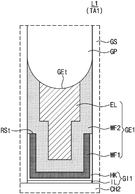
a gate electrode on the active fin; and
a gate insulating layer between the active fin and the gate electrode,
the gate insulating layer of the pull-down transistor comprises a first dipole element, and
a highest concentration of the first dipole element of the gate insulating layer of the pull-down transistor is higher than a highest concentration of the first dipole element of the gate insulating layer of the pass-gate transistor.
|