| CPC H04N 25/772 (2023.01) [H04N 25/709 (2023.01)] | 18 Claims |

|
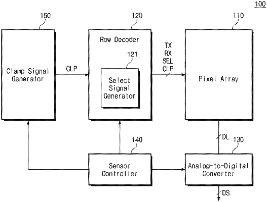
1. An image sensor device comprising:
a first image pixel connected to a first data line;
a second image pixel connected to the first data line;
an analog-to-digital converter configured to generate a digital signal based on a ramp signal and a voltage level of the first data line; and
a clamp signal generator configured to generate a clamp signal depending on an analog gain of the analog-to-digital converter,
wherein, while a data voltage is provided from the first image pixel to the first data line, the second image pixel provides a clamp voltage to the first data line based on the clamp signal, and while the data voltage is provided from the first image pixel to the first data line, a first select transistor of the first image pixel operates in a triode region, and a second select transistor of the second image pixel operates in a saturation region.
|