| CPC H03K 19/17748 (2013.01) [H03K 19/20 (2013.01)] | 10 Claims |

|
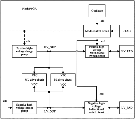
1. A configuration circuit of a flash field programmable gate array (FPGA) for realizing external monitoring and configuration, wherein the flash FPGA comprises a positive high-voltage external monitoring port and a negative high-voltage external monitoring port; the configuration circuit comprises a voltage supply circuit, a word line (WL) drive circuit, and a bit line (BL) drive circuit, wherein a positive output end of the voltage supply circuit is connected to positive voltage ends of the WL drive circuit and the BL drive circuit, and a negative output end of the voltage supply circuit is connected to negative voltage ends of the WL drive circuit and the BL drive circuit; wherein in the voltage supply circuit of the flash FPGA:
an oscillator is connected to clock signal terminals of a positive high-voltage charge pump and a negative high-voltage charge pump through a mode control circuit, and the mode control circuit further outputs a switch control signal to control on/off of a positive high-voltage bidirectional switch circuit and a negative high-voltage bidirectional switch circuit;
a positive high-voltage output terminal of the positive high-voltage charge pump is connected to the positive high-voltage external monitoring port through the positive high-voltage bidirectional switch circuit, and a common end of the positive high-voltage charge pump and the positive high-voltage bidirectional switch circuit is configured as the positive output end of the voltage supply circuit;
a negative high-voltage output terminal of the negative high-voltage charge pump is connected to the negative high-voltage external monitoring port through the negative high-voltage bidirectional switch circuit, and a common end of the negative high-voltage charge pump and the negative high-voltage bidirectional switch circuit is configured as the negative output end of the voltage supply circuit; and
the mode control circuit obtains a mode adjustment signal based on a Joint Test Action Group (JTAG) protocol of the flash FPGA and controls on/off of paths between the oscillator and the clock signal terminals of the positive high-voltage charge pump and the negative high-voltage charge pump and on/off of the positive high-voltage bidirectional switch circuit and the negative high-voltage bidirectional switch circuit based on the mode adjustment signal to control the flash FPGA to enter an external monitoring mode or an external configuration mode, wherein
in the external monitoring mode, a positive high voltage provided by the positive high-voltage charge pump is externally monitored through the positive high-voltage external monitoring port, and a negative high voltage provided by the negative high-voltage charge pump is externally monitored through the negative high-voltage external monitoring port; and
in the external configuration mode, an external positive high voltage is input through the positive high-voltage external monitoring port and output through the positive output end of the voltage supply circuit, and an external negative high voltage is input through the negative high-voltage external monitoring port and output through the negative output end of the voltage supply circuit.
|