US 12,095,010 B2
Light emitting diode and fabrication method thereof
Cheng Meng, Xiamen (CN); Yuehua Jia, Xiamen (CN); Jing Wang, Xiamen (CN); Chun-Yi Wu, Xiamen (CN); Ching-Shan Tao, Xiamen (CN); and Duxiang Wang, Xiamen (CN)
Assigned to XIAMEN SANAN OPTOELECTRONICS TECHNOLOGY CO., LTD., Xiamen (CN)
Filed by XIAMEN SANAN OPTOELECTRONICS TECHNOLOGY CO., LTD., Xiamen (CN)
Filed on Oct. 31, 2022, as Appl. No. 18/051,182.
Application 18/051,182 is a continuation of application No. 16/888,966, filed on Jun. 1, 2020, granted, now 11,522,107.
Application 16/888,966 is a continuation in part of application No. 16/522,634, filed on Jul. 25, 2019, granted, now 10,707,381.
Application 16/522,634 is a continuation of application No. 16/101,198, filed on Aug. 10, 2018, granted, now 10,411,163.
Application 16/101,198 is a continuation of application No. 15/647,127, filed on Jul. 11, 2017, granted, now 10,050,181.
Application 15/647,127 is a continuation of application No. PCT/CN2015/097539, filed on Dec. 16, 2015.
Claims priority of application No. 201510097522.2 (CN), filed on Mar. 5, 2015; application No. 201711476546.4 (CN), filed on Dec. 29, 2017; application No. 201721898534.6 (CN), filed on Dec. 29, 2017; and application No. 201721898549.2 (CN), filed on Dec. 29, 2017.
Prior Publication US 2023/0092504 A1, Mar. 23, 2023
This patent is subject to a terminal disclaimer.
Int. Cl. H01L 33/40 (2010.01); H01L 33/00 (2010.01); H01L 33/30 (2010.01); H01L 33/38 (2010.01); H01L 33/42 (2010.01); H01L 33/44 (2010.01)
CPC H01L 33/405 (2013.01) [H01L 33/0093 (2020.05); H01L 33/38 (2013.01); H01L 33/42 (2013.01); H01L 33/44 (2013.01); H01L 33/30 (2013.01); H01L 2933/0016 (2013.01); H01L 2933/0025 (2013.01)] 20 Claims
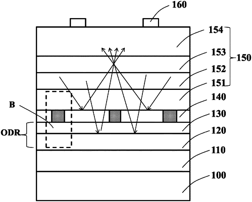
OG exemplary drawing
 
1. A light-emitting device (LED), comprising:
a light-emitting epitaxial layer having a first surface as a light-emitting surface and a second surface opposing the first surface, the light-emitting epitaxial layer including a first type semiconductor layer, an active layer, and a second type semiconductor layer;
a transparent dielectric layer located on the second surface and in direct contact with the light-emitting epitaxial laminated layer, and having conductive through-holes therein;
a transparent conductive layer located on one side surface of the transparent dielectric layer that is distal from the light-emitting epitaxial laminated layer; and
a metal reflective layer located on one side surface of the transparent conductive layer that is distal from the transparent dielectric layer;
wherein the transparent dielectric layer includes a first layer and a second layer; and
wherein the first layer is thicker than the second layer, and a refractivity of the first layer is less than a refractivity of the second layer.