| CPC H01L 28/65 (2013.01) [G11C 11/4023 (2013.01); H10B 12/30 (2023.02)] | 16 Claims |

|
1. A capacitor structure comprising:
a lower electrode;
an upper electrode; and
a capacitor dielectric film between the lower electrode and the upper electrode,
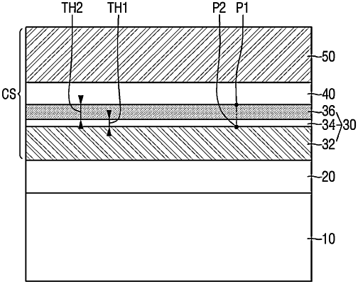
wherein the lower electrode includes an electrode film including a first metal element, and the lower electrode includes a doping oxide film including an oxide of the first metal element between the electrode film and the capacitor dielectric film,
the doping oxide film further includes a second metal element including an impurity element including at least one of silicon (Si), aluminum (Al), zirconium (Zr) and hafnium (Hf), and the doping oxide film includes at least one of Group 5 to Group 11 or Group 15 metal elements,
the lower electrode further includes a metal oxide film including an oxide of the first metal element and not including the second metal element,
the metal oxide film is between the electrode film and the doping oxide film,
the metal oxide film has a first thickness, and
the doping oxide film has a second thickness that is larger than the first thickness.
|