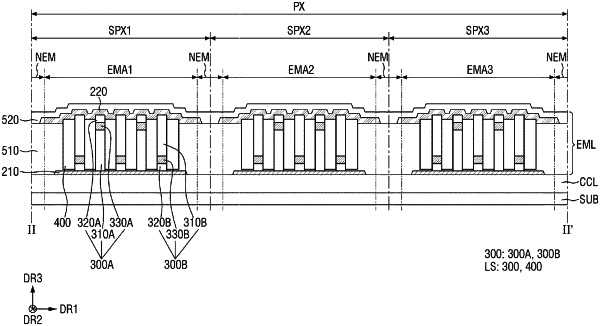
| CPC H01L 27/156 (2013.01) [H01L 33/24 (2013.01); H01L 33/54 (2013.01)] | 12 Claims |

|
1. A display device comprising:
a substrate;
a first electrode on the substrate;
a second electrode above the first electrode and spaced apart from the first electrode in a thickness direction of the substrate; and
a first unit of light-emitting elements and a second unit of light-emitting elements spaced apart from the first unit of light-emitting elements, the first and second units of light-emitting elements being between the first electrode and the second electrode,
wherein each of the first and second units unit of light-emitting elements comprises:
a plurality of light-emitting elements having a shape extended in a first direction and spaced apart from one another in a second direction perpendicular to the first direction, and
a binder extending around a periphery of the plurality of light-emitting elements and fixing the plurality of light-emitting elements,
wherein each of the plurality of light-emitting elements comprises a first semiconductor layer having one of an n-type or p-type conductivity, a second semiconductor layer having the other of the n-type or p-type conductivity, and an active layer between the first semiconductor layer and the second semiconductor layer,
wherein the plurality of light-emitting elements comprises:
a plurality of first light-emitting elements in which the first semiconductor layer, the active layer, and the second semiconductor layer are arranged along the first direction in this order, and
a plurality of second light-emitting elements in which the second semiconductor layer, the active layer, and the first semiconductor layer are arranged along the first direction in this order,
wherein the number of the plurality of first light-emitting elements is the same as the number of the plurality of second light-emitting elements in each of the first and second units of light-emitting elements, and
wherein the plurality of light-emitting elements in the first unit of light-emitting elements overlaps with the first electrode, and
wherein a first group of light-emitting elements from among the plurality of light-emitting elements in the second unit of light-emitting elements overlap with the first electrode and a second group of the light-emitting elements from among the plurality of light-emitting elements in the second unit of light-emitting elements do not overlap with the first electrode.
|