| CPC H01L 27/0924 (2013.01) [H01L 21/823821 (2013.01); H01L 21/823871 (2013.01); H01L 29/0673 (2013.01); H01L 29/0847 (2013.01); H01L 29/1037 (2013.01); H01L 29/167 (2013.01); H01L 29/4966 (2013.01); H01L 29/518 (2013.01); H01L 29/66545 (2013.01); H01L 29/785 (2013.01); H01L 2029/7858 (2013.01)] | 17 Claims |

|
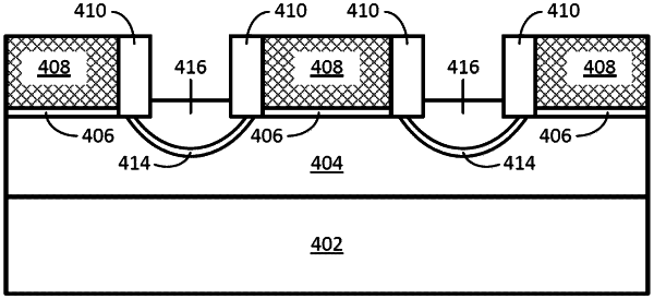
1. An integrated circuit structure, comprising:
a bulk silicon substrate;
a gate structure over the bulk silicon substrate, the gate structure being part of an NMOS transistor device; and
a source region and a drain region to respective sides of the gate structure, the source region and the drain region each being a bi-layer structure including a first layer and a second layer, wherein the first layer includes an arsenic concentration in a range of 1E20 atoms per cm3 to 5E21 atoms per cm3, and the second layer includes semiconductor fill.
|