| CPC H01L 23/5384 (2013.01) [H01L 21/4853 (2013.01); H01L 21/486 (2013.01); H01L 21/76802 (2013.01); H01L 23/5385 (2013.01); H01L 23/5386 (2013.01); H01L 24/14 (2013.01)] | 20 Claims |

|
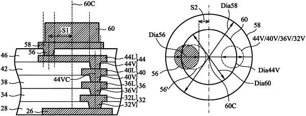
1. A method comprising:
forming a first dielectric layer;
forming a first redistribution line comprising a first via extending into the first dielectric layer, and a first trace over the first dielectric layer;
forming a second dielectric layer covering the first redistribution line;
patterning the second dielectric layer to form a via opening, wherein the first redistribution line is revealed through the via opening;
depositing a metal seed layer, wherein a part of the metal seed layer extends into the via opening;
plating a conductive material into the via opening and on the metal seed layer to form a second via in the second dielectric layer, and a conductive pad over and contacting the second via;
forming a plating mask covering and contacting the metal seed layer and a top surface of a peripheral portion of the conductive pad, wherein an additional portion of the conductive pad is exposed through the plating mask;
plating a conductive bump over the conductive pad, wherein the conductive bump is plated using the metal seed layer, wherein the second via is offset from a center line of the conductive bump;
removing the plating mask;
bonding a package component over the conductive bump; and
dispensing an underfill, wherein the underfill contacts a first sidewall of the conductive bump, and the underfill further contacts the top surface and a second sidewall of the conductive pad.
|