| CPC H01L 21/823418 (2013.01) [H01L 21/823431 (2013.01); H01L 27/0886 (2013.01); H01L 29/66795 (2013.01); H01L 29/7851 (2013.01)] | 20 Claims |

|
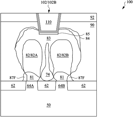
1. A method of forming a fin field-effect transistor (FinFET) device, the method comprising:
forming a first fin and a second fin that protrude above a substrate;
forming a gate structure over the first fin and the second fin;
forming, on a first side of the gate structure, a first recess and a second recess in the first fin and the second fin, respectively; and
forming a source/drain region in the first recess and the second recess, comprising:
forming a barrier layer in the first recess and the second recess;
forming a first epitaxial material over the barrier layer in the first recess and the second recess, wherein a first portion of the first epitaxial material over the first fin is spaced apart from a second portion of the first epitaxial material over the second fin;
forming a second epitaxial material over the first epitaxial material, wherein the second epitaxial material extends along exterior surfaces of the first portion and the second portion of the first epitaxial material, wherein the second epitaxial material extends continuously from the first fin to the second fin; and
forming a capping layer over the second epitaxial material, wherein each of the first epitaxial material, the second epitaxial material, and the capping layer comprises a semiconductor material and a dopant, wherein a second concentration of the dopant in the second epitaxial material is higher than a first concentration of the dopant in the first epitaxial material, wherein a third concentration of the dopant in the capping layer is lower than the first concentration of the dopant in the first epitaxial material.
|