| CPC H01L 21/0332 (2013.01) [H01L 21/02175 (2013.01); H01L 21/02565 (2013.01); H01L 21/0262 (2013.01); H01L 21/0274 (2013.01); H01L 21/0337 (2013.01); H01L 21/3065 (2013.01); H01L 21/31116 (2013.01); H01L 21/31122 (2013.01); H01L 21/31138 (2013.01); H01L 21/31144 (2013.01); H01L 21/32136 (2013.01); H01L 21/32137 (2013.01); H01L 21/32139 (2013.01); H01L 21/465 (2013.01); H01L 21/467 (2013.01); H01L 21/67069 (2013.01); H01L 21/67167 (2013.01); H01L 21/67207 (2013.01); H01J 37/3211 (2013.01); H01J 37/32651 (2013.01); H01J 2237/186 (2013.01); H01J 2237/3321 (2013.01); H01J 2237/334 (2013.01); H01L 21/02205 (2013.01); H01L 21/02274 (2013.01); H01L 21/0228 (2013.01); H01L 21/68 (2013.01); H01L 21/6833 (2013.01)] | 18 Claims |

|
1. A system for processing a semiconductor substrate, the system comprising:
(a) one or more deposition chambers;
(b) one or more etch chambers;
(c) a plasma generator and
(d) a controller comprising program instructions configured to cause:
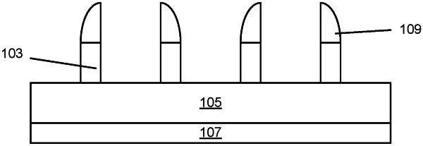
(i) a deposition of a tin oxide layer on the semiconductor substrate, wherein the deposition comprises exposing the semiconductor substrate to a tin-containing precursor and an oxygen-containing precursor; and
(ii) a contact of the semiconductor substrate with a plasma formed in a process gas comprising H2 and a hydrocarbon, such that a carbon-containing polymer is formed on the semiconductor substrate, wherein a ratio of H2 to hydrocarbon in the process gas is at least 5, thereby causing selective etching of the tin oxide layer in a presence of a material selected from the group consisting of silicon (Si), carbon (C), and a carbon-containing material with an etch selectivity of at least 10.
|