| CPC H01L 21/0234 (2013.01) [H01L 21/02164 (2013.01); H01L 21/0223 (2013.01); H01L 21/02271 (2013.01)] | 20 Claims |

|
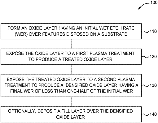
1. A method for processing a substrate, comprising:
forming an oxide layer comprising silicon oxide and having an initial wet etch rate (WER) over features disposed on the substrate, wherein the initial WER is determined with an etchant having a concentration;
exposing the oxide layer to a first plasma treatment to produce a treated oxide layer while maintaining the substrate at a first temperature of less than 600° C., wherein the first plasma treatment comprises:
generating a first plasma by a first RF source; and
directing the first plasma to the oxide layer by a DC bias; and then
exposing the treated oxide layer to a second plasma treatment to produce a densified oxide layer while maintaining the substrate at a second temperature of less than 600° C., wherein the densified oxide layer has a final WER of less than one-half of the initial WER, wherein the final WER is determined with the etchant having the concentration, wherein the oxide layer comprising silicon oxide has a normalized wet etch rate ratio (WERR) of 1 and the densified oxide layer has a final WERR of about 0.1 to about 0.48, and wherein the second plasma treatment comprises:
generating a second plasma by a top RF source and a side RF source; and
directing the second plasma to the treated oxide layer without a bias.
|