| CPC G11C 7/1006 (2013.01) [G11C 7/1048 (2013.01); G11C 11/4093 (2013.01); G11C 11/4096 (2013.01); H03K 19/0185 (2013.01)] | 10 Claims |

|
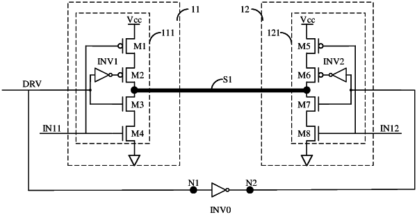
1. A signal line structure, comprising:
a plurality of parallel signal lines, wherein each of the signal lines is maintained in a drive state at any time; and,
wherein two ends of each of the signal lines are respectively connected to a first driver and a second driver, and at the same time, only one of the first driver and the second driver of the same signal line is maintained in a drive state; and,
the first driver is maintained in the drive state when a first enable signal is at a first level and maintained in a high-impedance state when the first enable signal is at a second level; and the second driver is maintained in the drive state when a second enable signal is at the first level and maintained in the high-impedance state when the second enable signal is at the second level; and,
the second enable signal is obtained by inverting the first enable signal through an inverter.
|