US 12,094,508 B1
Magnetic tunneling junction switching with parallel spin-momentum locked spin current
See-Hun Yang, San Jose, CA (US); Mahesh Govind Samant, San Jose, CA (US); Panagiotis Charilaos Filippou, San Jose, CA (US); Chirag Garg, San Jose, CA (US); Fnu Ikhtiar, San Jose, CA (US); and Jaewoo Jeong, San Jose, CA (US)
Assigned to Samsung Electronics Co., Ltd., (KR)
Filed by Samsung Electronics Co., Ltd., Gyeonggi-do (KR); and INTERNATIONAL BUSINESS MACHINES CORPORATION, Armonk, NY (US)
Filed on Nov. 15, 2023, as Appl. No. 18/509,818.
Int. Cl. G11C 11/16 (2006.01); H01F 10/32 (2006.01); H10B 61/00 (2023.01); H10N 50/01 (2023.01); H10N 50/10 (2023.01); H10N 50/85 (2023.01)
CPC G11C 11/161 (2013.01) [H01F 10/329 (2013.01); H10B 61/00 (2023.02); H10N 50/01 (2023.02); H10N 50/10 (2023.02); H10N 50/85 (2023.02)] 17 Claims
OG exemplary drawing
 
1. A device, comprising:
a substrate;
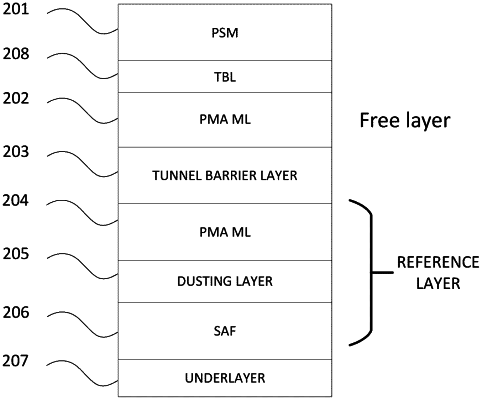
a magnetic tunnel junction (MTJ) formed over the substrate, the MTJ including a reference layer, a tunnel barrier layer, and a free layer;
a parallel spin-momentum (PSM) layer formed over the free layer of the MTJ, the PSM layer including a chiral material; and
a texture breaking layer (TBL) formed between the free layer of the MTJ and the PSM layer.