| CPC G06F 30/347 (2020.01) [G06F 30/31 (2020.01); G06F 30/392 (2020.01); G06F 15/7825 (2013.01)] | 20 Claims |

|
1. A method comprising:
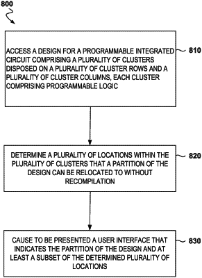
accessing, by one or more processors, a design for a programmable integrated circuit comprising a plurality of clusters disposed on a plurality of cluster rows and a plurality of cluster columns, each cluster comprising programmable logic and a network on chip (NoC) endpoint;
accessing, by the one or more processors, a selection of a selected portion of the design, that is within a cluster of the plurality of clusters and located at a determined offset from the NoC endpoint of the cluster;
determining, by the one or more processors, a plurality of locations within the plurality of clusters that the selected portion of the design can be relocated to without recompilation based on the determined offset; and
causing to be presented, by the one or more processors, a user interface that indicates the selected portion of the design and at least a subset of the determined plurality of locations.
|