US 12,092,935 B2
Display panel and method of manufacturing the same
Jin-Soo Jung, Hwaseong-si (KR); Young Gu Kim, Hwaseong-si (KR); Byoung-Hun Sung, Hwaseong-si (KR); and Baekkyun Jeon, Yongin-si (KR)
Assigned to SAMSUNG DISPLAY CO., LTD., Yongin (KR)
Filed by SAMSUNG DISPLAY CO., LTD., Yongin-si (KR)
Filed on Jul. 18, 2023, as Appl. No. 18/223,248.
Application 15/078,636 is a division of application No. 13/830,766, filed on Mar. 14, 2013, granted, now 9,329,447, issued on May 3, 2016.
Application 18/223,248 is a continuation of application No. 17/580,912, filed on Jan. 21, 2022, granted, now 11,740,520.
Application 17/580,912 is a continuation of application No. 16/790,402, filed on Feb. 13, 2020, granted, now 11,262,630, issued on Mar. 1, 2022.
Application 16/790,402 is a continuation of application No. 15/828,645, filed on Dec. 1, 2017, granted, now 10,578,939, issued on Mar. 3, 2020.
Application 15/828,645 is a continuation of application No. 15/078,636, filed on Mar. 23, 2016, granted, now 9,835,918, issued on Dec. 5, 2017.
Claims priority of application No. 10-2012-0066249 (KR), filed on Jun. 20, 2012.
Prior Publication US 2023/0359095 A1, Nov. 9, 2023
Int. Cl. G02F 1/1345 (2006.01); F21V 8/00 (2006.01); G02F 1/1333 (2006.01); G02F 1/1339 (2006.01); G02F 1/1362 (2006.01); G02F 1/1368 (2006.01); H01L 33/08 (2010.01)
CPC G02F 1/136286 (2013.01) [G02B 6/0083 (2013.01); G02F 1/133345 (2013.01); G02F 1/1339 (2013.01); G02F 1/13452 (2013.01); G02F 1/136227 (2013.01); G02F 1/1368 (2013.01); H01L 33/08 (2013.01); G02F 1/13458 (2013.01); H01L 2924/0002 (2013.01)] 10 Claims
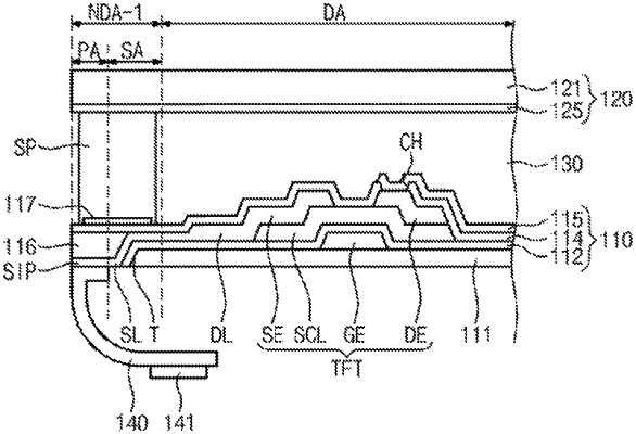
OG exemplary drawing
 
1. A display panel comprising:
a base substrate including an upper surface and a lower surface facing the upper surface, wherein the upper surface includes a display area and a non-display area which is adjacent to the display area;
an organic polymer layer on the non-display area;
a pixel on the upper surface and in the display area;
a signal input pad on the organic polymer layer;
a signal line which connects the signal input pad with the pixel;
a flexible printed circuit board connected to the signal input pad; and
a driver Integrated Circuit mounted on the flexible printed circuit board and overlapping the display area in a plan view,
wherein the flexible printed circuit board is disposed between the driver integrated circuit and the lower surface within a cross sectional view.