US 12,092,932 B2
Liquid crystal display device
Yasushi Tomioka, Tokyo (JP); Yosuke Hyodo, Tokyo (JP); Hidehiro Sonoda, Tokyo (JP); and Noboru Kunimatsu, Tokyo (JP)
Assigned to Japan Display Inc., Tokyo (JP)
Filed by Japan Display Inc., Tokyo (JP)
Filed on Jan. 10, 2024, as Appl. No. 18/408,683.
Application 18/408,683 is a continuation of application No. 18/140,006, filed on Apr. 27, 2023, granted, now 11,906,857.
Application 18/140,006 is a continuation of application No. 17/946,602, filed on Sep. 16, 2022, granted, now 11,668,982, issued on Jun. 6, 2023.
Application 17/946,602 is a continuation of application No. 17/475,403, filed on Sep. 15, 2021, granted, now 11,480,833, issued on Oct. 25, 2022.
Application 17/475,403 is a continuation of application No. 16/953,997, filed on Nov. 20, 2020, granted, now 11,150,523, issued on Oct. 19, 2021.
Application 16/953,997 is a continuation of application No. 16/273,586, filed on Feb. 12, 2019, granted, now 10,877,325, issued on Dec. 29, 2020.
Application 16/273,586 is a continuation of application No. 16/158,402, filed on Oct. 12, 2018, granted, now 10,247,990, issued on Apr. 2, 2019.
Application 16/158,402 is a continuation of application No. 16/014,024, filed on Jun. 21, 2018, granted, now 10,126,611, issued on Nov. 13, 2018.
Application 16/014,024 is a continuation of application No. 15/891,707, filed on Feb. 8, 2018, granted, now 10,031,383, issued on Jul. 24, 2018.
Application 15/891,707 is a continuation of application No. 15/693,564, filed on Sep. 1, 2017, granted, now 9,921,440, issued on Mar. 20, 2018.
Application 15/693,564 is a continuation of application No. 15/401,795, filed on Jan. 9, 2017, granted, now 9,778,520, issued on Oct. 3, 2017.
Application 15/401,795 is a continuation of application No. 15/212,873, filed on Jul. 18, 2016, granted, now 9,575,385, issued on Feb. 21, 2017.
Application 15/212,873 is a continuation of application No. 14/978,671, filed on Dec. 22, 2015, granted, now 9,417,496, issued on Aug. 16, 2016.
Application 14/978,671 is a continuation of application No. 14/527,841, filed on Oct. 30, 2014, granted, now 9,250,491, issued on Feb. 2, 2016.
Claims priority of application No. 2013-226910 (JP), filed on Oct. 31, 2013.
Prior Publication US 2024/0142830 A1, May 2, 2024
Int. Cl. G02F 1/1343 (2006.01); G02F 1/1333 (2006.01); G02F 1/1335 (2006.01); G02F 1/1337 (2006.01); G02F 1/1362 (2006.01); G02F 1/1368 (2006.01); H01L 27/12 (2006.01)
CPC G02F 1/134363 (2013.01) [G02F 1/133345 (2013.01); G02F 1/133512 (2013.01); G02F 1/133514 (2013.01); G02F 1/133788 (2013.01); G02F 1/136227 (2013.01); G02F 1/1368 (2013.01); H01L 27/1218 (2013.01); G02F 2202/02 (2013.01)] 9 Claims
OG exemplary drawing
 
1. A display device comprising:
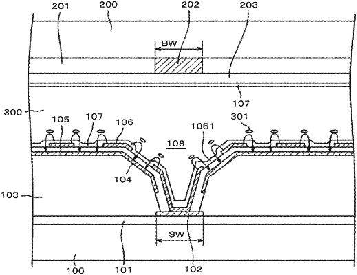
a first substrate including an organic insulation layer, a first electrode on the organic insulation layer, an inorganic insulating layer on the first electrode, a second electrode on the inorganic insulating layer, a photo-alignment layer on the inorganic insulating layer and the second electrode, and a metal layer between the substrate and the organic insulation layer;
a second substrate; and
a liquid crystal material between the first substrate and the second substrate,
wherein
the organic insulation layer has a through hole, and the second electrode connects the metal layer via the through hole,
the second electrode has a slit,
a part of the second electrode, a part of the photo-alignment layer, and a part of the slit are positioned in the through hole, and
the through hole has a portion that has a diameter which is larger than a width of the metal layer.