US 12,092,839 B2
Multifunctional collimator for contact image sensors
Hsin-Yu Chen, Hsinchu (TW); Chun-Peng Li, Hsinchu (TW); Chia-Chun Hung, Hsinchu (TW); Ching-Hsiang Hu, Taipei (TW); Wei-Ding Wu, Zhubei (TW); Jui-Chun Weng, Taipei (TW); Ji-Hong Chiang, Changhua (TW); Yen Chiang Liu, Hsinchu (TW); Jiun-Jie Chiou, Hsinchu (TW); Li-Yang Tu, Hsinchu (TW); Jia-Syuan Li, Hsinchu (TW); You-Cheng Jhang, Hsinchu (TW); Shin-Hua Chen, Hsinchu (TW); Lavanya Sanagavarapu, Hsinchu (TW); Han-Zong Pan, Hsinchu (TW); and Hsi-Cheng Hsu, Taichung (TW)
Assigned to Taiwan Semiconductor Manufacturing Co., Ltd., Hsin-Chu (TW)
Filed by Taiwan Semiconductor Manufacturing Co., Ltd., Hsin-Chu (TW)
Filed on Jul. 14, 2023, as Appl. No. 18/222,344.
Application 18/222,344 is a continuation of application No. 17/881,439, filed on Aug. 4, 2022, granted, now 11,726,342.
Application 17/881,439 is a continuation of application No. 16/655,763, filed on Oct. 17, 2019, granted, now 11,448,891.
Prior Publication US 2023/0359056 A1, Nov. 9, 2023
This patent is subject to a terminal disclaimer.
Int. Cl. G02B 27/30 (2006.01); H01L 27/146 (2006.01); H01L 31/0232 (2014.01)
CPC G02B 27/30 (2013.01) [H01L 27/14625 (2013.01); H01L 31/02325 (2013.01)] 20 Claims
OG exemplary drawing
 
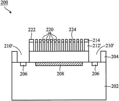
1. An optical collimator, comprising:
a dielectric layer;
a substrate; and
a plurality of via holes,
wherein the dielectric layer is formed over the substrate, wherein each of the plurality of via holes extends through the dielectric layer and the substrate from a first surface of the dielectric layer to a second surface of the substrate in a vertical direction, wherein a first thickness of the substrate is equal to or greater than 75 micrometers, a second thickness of the dielectric layer is in a range of 1.5-2.5 micrometers, and the optical collimator is configured to filter light in a range of wavelengths.