| CPC G01R 29/0878 (2013.01) [G01R 29/0892 (2013.01)] | 23 Claims |

|
1. A method of testing a semiconductor device, comprising:
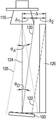
disposing an antenna-in-package (AiP) module under a test antenna of a testing system;
calibrating the testing system by,
transmitting a first signal with a first antenna of the AiP module,
moving the test antenna to find a power output peak of the first signal,
storing coordinates of the power output peak of the first signal for both a first directional axis and a second directional axis,
discontinuing transmission of the first signal with the first antenna,
transmitting a second signal with a second antenna of the AiP module after discontinuing transmission of the first signal with the first antenna,
moving the test antenna along the first directional axis from the power output peak of the first signal to a power output peak of the second signal while a position of the test antenna along the second directional axis is held static, and
storing only a first coordinate along the first directional axis for the power output peak of the second signal; and
testing the AiP module after calibrating the testing system by,
returning the test antenna to the stored coordinates for the power output peak of the first signal,
testing the first antenna of the AiP module while the test antenna is at the power output peak of the first signal,
moving the test antenna along the first directional axis to the stored first coordinate for the power output peak for the second signal, and
testing the second antenna of the AiP module while the test antenna is at the power output peak of the second signal.
|
|
6. A method of testing a semiconductor device, comprising:
disposing an antenna-in-package (AiP) module under a test antenna;
transmitting a first signal with a first antenna of the AiP module;
moving the test antenna to a power output peak of the first signal;
storing coordinates of the power output peak of the first signal for both a first directional axis and a second directional axis,
discontinuing transmission of the first signal;
transmitting a second signal with a second antenna of the AiP module after discontinuing transmission of the first signal;
moving the test antenna along a first directional axis to a power output peak of the second signal while a second directional axis of the test antenna is held static; and
storing only a first coordinate along the first directional axis for the power output peak of the second signal.
|
|
12. A method of testing a semiconductor device, comprising:
disposing an antenna-in-package (AiP) module under a test antenna of a testing system;
calibrating the testing system by,
transmitting a first signal with a first antenna of the AiP module while a second antenna of the AiP module is not transmitting, and
moving the test antenna to a power output peak of the first signal while the first antenna is transmitting the first signal and while the second antenna of the AiP module is not transmitting,
discontinuing transmission of the first signal with the first antenna,
transmitting a second signal with a second antenna of the AiP module after discontinuing transmission of the first signal with the first antenna, and
moving the test antenna to a power output peak of the second signal while the second antenna is transmitting the second signal; and
testing the AiP module after calibrating the testing system by,
returning the test antenna to the power output peak of the first signal,
testing the first antenna of the AiP module while the test antenna is at the power output peak of the first signal,
moving the test antenna to the power output peak for the second signal, and
testing the second antenna of the AiP module while the test antenna is at the power output peak of the second signal.
|
|
19. A semiconductor testing device, comprising:
a motorized fixture;
a test antenna mounted to an arm of the motorized fixture;
an antenna-in-package (AiP) module disposed under the test antenna; and
a computer configured to calibrate the testing system by,
transmitting a first signal with a first antenna of the AiP module,
moving the test antenna to find a power output peak of the first signal,
storing coordinates of the power output peak of the first signal for both a first directional axis and a second directional axis,
discontinuing transmission of the first signal with the first antenna,
transmitting a second signal with a second antenna of the AiP module after discontinuing transmission of the first signal with the first antenna,
moving the test antenna along the first directional axis from the power output peak of the first signal to a power output peak of the second signal while a position of the test antenna along the second directional axis is held static, and
storing only a first coordinate along the first directional axis for the power output peak of the second signal;
wherein the computer is configured to test the AiP module by,
returning the test antenna to the stored coordinates for the power output peak of the first signal,
testing the first antenna of the AiP module while the test antenna is at the power output peak of the first signal,
moving the test antenna along the first directional axis to the stored first coordinate for the power output peak for the second signal, and
testing the second antenna of the AiP module while the test antenna is at the power output peak of the second signal.
|