| CPC H10N 50/10 (2023.02) [H10B 61/00 (2023.02); H10N 50/80 (2023.02); H10N 50/85 (2023.02)] | 14 Claims |

|
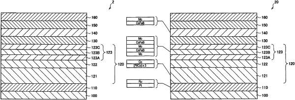
1. A magnetoresistance effect element comprising: a first electrode;
a magnetization pinned layer that is provided on the first electrode and has a fixed magnetization direction;
a first insulating layer provided on the magnetization pinned layer;
a magnetization free layer that is provided on the first insulating layer and has a variable magnetization direction;
a second insulating layer provided on the magnetization free layer; and
a second electrode provided on the second insulating layer,
wherein
the magnetization pinned layer includes a first magnetic body provided on the first electrode, and a second magnetic body provided on the first magnetic body via a non-magnetic metal layer,
at least any of the first magnetic body and the second magnetic body is configured by providing a magnetic layer directly above a non-magnetic layer, and
the non-magnetic layer is formed in a multilayer structure in which different materials are alternately laminated.
|