| CPC H10K 59/65 (2023.02) [G06F 3/0412 (2013.01); H10K 50/844 (2023.02); H10K 59/122 (2023.02); H10K 59/131 (2023.02); H10K 59/40 (2023.02); G02F 1/133305 (2013.01); G06F 1/1652 (2013.01); G09F 9/301 (2013.01); G09G 2300/0408 (2013.01); G09G 2300/0804 (2013.01); G09G 2380/02 (2013.01); H01L 27/14678 (2013.01); H01L 33/12 (2013.01); H10K 50/816 (2023.02); H10K 50/828 (2023.02); H10K 59/1213 (2023.02); H10K 59/1216 (2023.02); H10K 59/123 (2023.02); H10K 59/35 (2023.02); H10K 59/353 (2023.02); H10K 77/111 (2023.02); H10K 2102/00 (2023.02); H10K 2102/311 (2023.02)] | 21 Claims |

|
1. A display device, comprising:
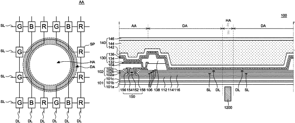
a flexible substrate having a pixel area and a see-through area within the pixel area;
a driving transistor, a switching transistor, and a data line disposed in the pixel area;
a first electrode, a second electrode, and an emission layer between the first electrode and the second electrode;
an encapsulation part over the substrate; and
a touch panel over the encapsulation part, the touch panel including a plurality of touch electrodes,
wherein a portion of at least one of the data line are curved in a routing area adjacent to the see-through area, and
wherein at least one touch electrode of the plurality of touch electrodes overlaps with the see-through area from a plan view.
|