| CPC H10K 59/131 (2023.02) [H01L 25/18 (2013.01); H10K 77/10 (2023.02); H01L 24/06 (2013.01); H01L 24/08 (2013.01); H01L 2224/0603 (2013.01); H01L 2224/08145 (2013.01); H10K 59/1201 (2023.02)] | 16 Claims |

|
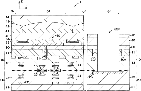
1. A display device, comprising:
a pixel that includes a light-emitting part;
a pad electrode;
a first substrate that includes a semiconductor material layer that includes a transistor, wherein the transistor is configured to drive the light-emitting part included in the pixel;
a second substrate that includes a specific circuit,
wherein a first surface of the first substrate joins a second surface of the second substrate such that the first surface faces the second surface;
an insulating film on the first substrate;
a first electrode on the insulating film, wherein the first electrode is arranged in a matrix shape;
an organic layer over an entire surface including an upper side of the first electrode;
a second electrode over an entire surface including an upper side of the organic layer,
wherein the insulating film, the first electrode, the organic layer, and the second electrode are stacked on the first substrate, and
the light-emitting part includes the first electrode, the organic layer, and the second electrode; and
a pad opening from a first side of the first substrate faces the pad electrode on a second side of each of a respective one of the first surface and the second surface, such that the pad electrode is exposed on a bottom surface, wherein
the pad opening penetrates the semiconductor material layer of the first substrate, and
the semiconductor material layer is around the pad opening sectioned by an insulating structure along a circumference of the pad opening on the second side of each of the respective one of the first surface and the second surface.
|