| CPC H10K 59/131 (2023.02) [H10K 59/122 (2023.02); H10K 59/124 (2023.02); H10K 59/126 (2023.02); H10K 59/352 (2023.02)] | 20 Claims |

|
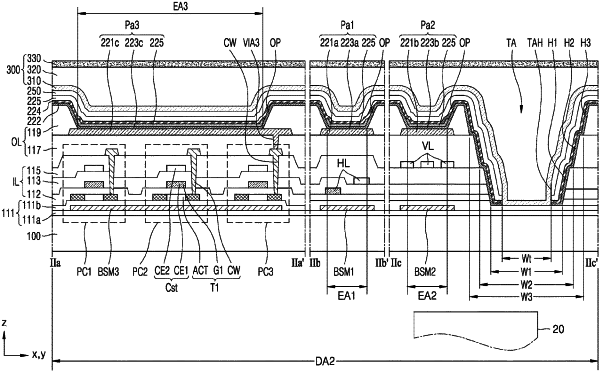
1. A display device comprising:
a first line group comprising first lines extending in a first direction on a substrate, in a plan view;
a second line group comprising second lines extending in a second direction on the substrate, the second direction intersecting the first direction in a plan view;
a pixel circuit disposed at a region where the first line group intersects the second line group;
a display element overlapping the pixel circuit;
a transmissive area surrounded by the first line group and the second line group and not overlapping the first line group or the second line group, in a plan view; and
a metal layer disposed between the substrate and the pixel circuit in a cross-sectional view, the metal layer comprising an opening corresponding to the transmissive area,
wherein the metal layer overlaps the first line group. the second line group, and the pixel circuit.
|