| CPC H10K 59/1275 (2023.02) [H10K 59/1201 (2023.02); H10K 59/1213 (2023.02); H10K 59/126 (2023.02); H10K 59/50 (2023.02); H10K 59/8792 (2023.02); H10K 77/111 (2023.02); H10K 2102/3031 (2023.02)] | 20 Claims |

|
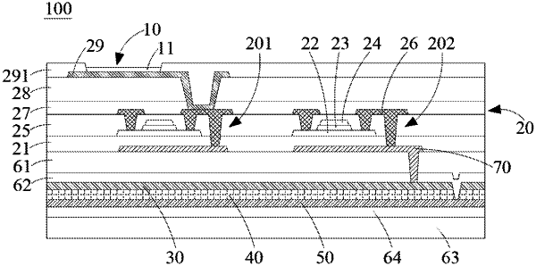
1. A double-sided display panel, which comprises:
a light-emitting device layer comprising a plurality of light-emitting devices;
a thin film transistor (TFT) layer disposed on a side of the light-emitting device layer, wherein the TFT layer comprises a first TFT and a second TFT, and the first TFT is electrically connected to one of the light-emitting devices;
a first light-shielding conductive layer disposed on a side of the TFT layer away from the light-emitting device layer, and electrically connected to the second TFT;
an electrochromic layer disposed on a side of the first light-shielding conductive layer away from the TFT layer, and electrically connected to the first light-shielding conductive layer; and
a light-transmitting conductive layer disposed on a side of the electrochromic layer away from the first light-shielding conductive layer, and electrically connected to the electrochromic layer.
|