| CPC H10K 59/122 (2023.02) [G06F 3/0416 (2013.01); G09G 3/3225 (2013.01); G09G 2300/0814 (2013.01); G09G 2300/0852 (2013.01); G09G 2320/0209 (2013.01); H01L 24/32 (2013.01); H01L 2224/32225 (2013.01); H10K 50/852 (2023.02); H10K 59/30 (2023.02)] | 18 Claims |

|
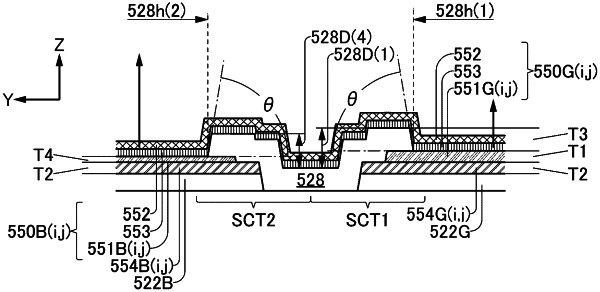
1. A functional panel comprising:
a first element comprising a first reflective film;
a second element comprising a second reflective film; and
an insulating film,
wherein the first element further comprises a first electrode, a second electrode, and a layer containing a light-emitting material,
wherein the insulating film is located over a portion of the first reflective film and a portion of the first electrode,
wherein the layer containing the light-emitting material comprises a region interposed between the first electrode and the second electrode,
wherein the first electrode has a light-transmitting property,
wherein the first electrode has a first thickness,
wherein the first electrode is interposed between a region of the first reflective film and the layer containing the light-emitting material,
wherein the first reflective film has a second thickness,
wherein the insulating film comprises a first opening portion,
wherein the first opening portion overlaps with the first electrode,
wherein the insulating film has a first step-like cross-sectional shape,
wherein the first step-like cross-sectional shape surrounds the first opening portion when seen from above,
wherein the first step-like cross-sectional shape comprises a first step,
wherein the second thickness is greater than the first thickness,
wherein the second reflective film has the second thickness, and
wherein the first reflective film comprises a region which extends beyond an end portion of the first electrode.
|