| CPC H10K 59/1213 (2023.02) [H10K 59/1216 (2023.02); H10K 59/131 (2023.02); G09G 3/3258 (2013.01); G09G 3/3266 (2013.01); G09G 2320/02 (2013.01); G09G 2330/00 (2013.01); H01L 27/1225 (2013.01); H01L 27/124 (2013.01); H01L 27/1251 (2013.01); H01L 27/1255 (2013.01); H01L 29/78675 (2013.01); H01L 29/7869 (2013.01)] | 19 Claims |

|
1. A display device comprising:
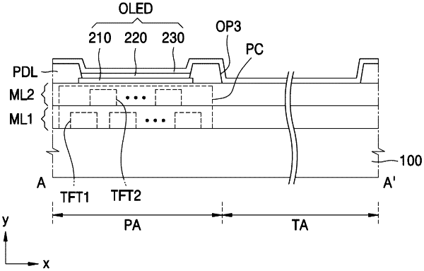
a substrate that includes a pixel area and a transmission area;
a pixel circuit disposed in the pixel area and comprising:
a first thin-film transistor included in a first multi-layer film; and
a second thin-film transistor included in a second multi-layer film on the first multi-layer film, the first thin-film transistor and the second thin-film transistor being electrically connected to each other; and
a display element disposed on the second multi-layer film and comprising:
a pixel electrode electrically connected to the second thin-film transistor via a contact hole defined in the second multi-layer film; and
a pixel-defining layer on the second multi-layer film including a first opening that exposes a portion of the pixel electrode and a second opening corresponding to the transmission area,
wherein each of the first multi-layer film and the second multi-layer film comprises a plurality of sub-layers, and
at least one of the plurality of sub-layers of the first multi-layer film or the second multi-layer film includes an opening below the second opening; wherein the first multi-layer film comprises a scan line and an emission control line that extend in a first direction, and the scan line and the emission control line bypass the transmission area.
|