| CPC H10K 59/1213 (2023.02) [H10K 59/1216 (2023.02); H10K 59/131 (2023.02); H10K 59/1201 (2023.02)] | 19 Claims |

|
1. An array substrate, comprising:
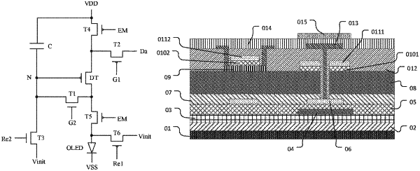
a pixel driving circuit, the pixel driving circuit comprising a P-type driving transistor, an N-type first transistor, and a capacitor, wherein a first electrode of the N-type first transistor is connected to a gate electrode of the P-type driving transistor, and a first electrode of the capacitor is connected to the gate electrode of the P-type driving transistor;
a base substrate;
a first conductive layer laminated at a side of the base substrate, the first conductive layer comprising a first conductive portion, and the first conductive portion being configured as the gate electrode of the P-type driving transistor and the first electrode of the capacitor;
a first dielectric layer laminated at a side of the first conductive layer facing away from the base substrate;
a first buffer layer laminated at a side of the first dielectric layer facing away from the base substrate, a slot being provided on the first buffer layer, and an orthographic projection of the slot on the base substrate being at least partially overlapped with an orthographic projection of the first conductive portion on the base substrate; and
a second conductive layer laminated at a side of the first buffer layer facing away from the base substrate, the second conductive layer comprising:
a second conductive portion configured as a gate electrode of the N-type first transistor; and
a third conductive portion at least partially at a bottom portion of the slot, an orthographic projection of the third conductive portion on the base substrate being at least partially overlapped with the orthographic projection of the first conductive portion on the base substrate, so as to form a second electrode of the capacitor.
|