| CPC H10B 43/27 (2023.02) [G11C 16/0483 (2013.01); G11C 16/06 (2013.01); H10B 43/40 (2023.02)] | 20 Claims |

|
1. A non-volatile memory device comprising:
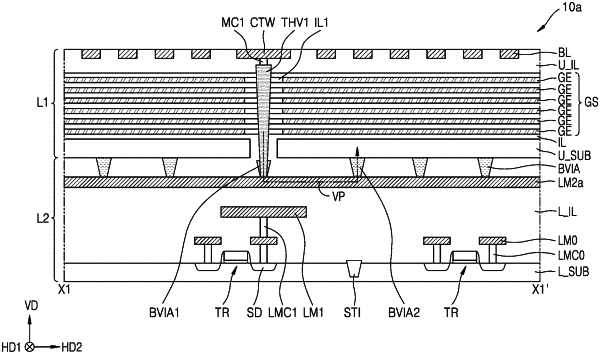
a memory cell region including an upper substrate, channel structures, and a first upper metal line, the channel structure extending in a vertical direction on the upper substrate, the first upper metal line extending in a first horizontal direction above the channel structures; and
a peripheral circuit region below the memory cell region in the vertical direction, the peripheral circuit region including a first lower metal line extending in a second horizontal direction, a first via structure on the first lower metal line, and a second via structure on the first lower metal line, a top surface of the second via structure being in contact with the upper substrate,
wherein the memory cell region further includes a first through-hole via structure, the first through-hole via structure extending in the vertical direction, the first through-hole via structure passing through the upper substrate and the first via structure, and the first through-hole via structure electrically connecting the first upper metal line to the first lower metal line, and
wherein the first upper metal line is electrically connected to the upper substrate through the first through-hole via structure, the first lower metal line, and the second via structure.
|