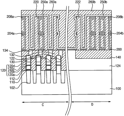
| CPC H10B 12/315 (2023.02) [H01L 28/92 (2013.01); H10B 12/50 (2023.02); H10B 12/0335 (2023.02); H10B 12/09 (2023.02)] | 20 Claims |

|
1. A semiconductor device, comprising:
a cell capacitor on a memory cell region of a substrate, the cell capacitor including a plurality of first lower electrodes, a first upper support layer pattern, a first dielectric layer, and a first upper electrode; and
a decoupling capacitor on a decoupling capacitor region of the substrate, the decoupling capacitor including a plurality of second lower electrodes, a second upper support layer pattern, a second dielectric layer, and a second upper electrode,
wherein the plurality of first and second lower electrodes are arranged in a honeycomb pattern, which is arranged at each vertex of a hexagon and a center of the hexagon,
the plurality of first and second lower electrodes correspond to rows extending along a first direction, and each of the rows are arranged in a second direction perpendicular to the first direction,
the first upper support layer pattern is connected to upper sidewalls of the plurality of first lower electrodes, the first upper support layer pattern is between the plurality of first lower electrodes, and the first upper support layer pattern corresponds to a first plate defining first openings, wherein all of the plurality of first lower electrodes are partially exposed by the first openings,
the second upper support layer pattern is connected to the upper sidewalls of the second lower electrodes, the second upper support layer pattern is between the plurality of second lower electrodes, and the second upper support layer pattern corresponds to a second plate defining second openings, wherein some of the plurality of second lower electrodes are partially exposed by the second openings, and some of the plurality of second lower electrodes are not exposed by the second openings.
|