| CPC H05K 9/0028 (2013.01) [G01R 15/04 (2013.01); G01R 19/10 (2013.01); H05K 1/0216 (2013.01)] | 14 Claims |

|
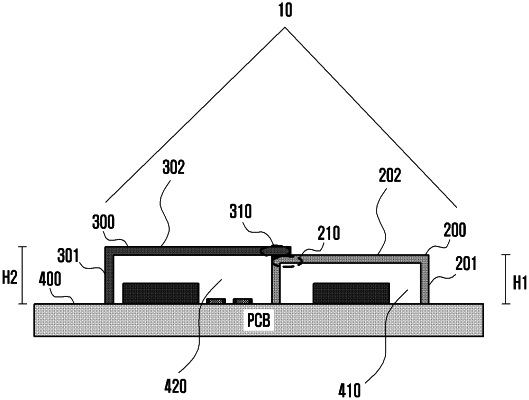
1. An electronic device comprising:
a substrate;
a first electronic component mounted on a first region of a surface of the substrate;
a second electronic component mounted on a second region of the surface of the substrate;
a first electromagnetic interference (EMI) shield configured to shield the first electronic component; and
a second EMI shield configured to shield the second electronic component,
wherein the first EMI shield includes a first shield cover and a first shield frame configured to surround the first electronic component between the first shield cover and the first region,
wherein the second EMI shield includes a second shield cover and a second shield frame, and
wherein the second shield frame and a portion of the first shield frame are configured to surround the second electronic component between the second shield cover and the second region.
|