US 12,089,331 B2
Metal circuit structure based on FPC and method of making the same
Cheng-Neng Chen, Changzhou (CN); Sui-Ho Tsai, Changzhou (CN); Yun-Nan Wang, Changzhou (CN); and Chiao-Hui Wang, Changzhou (CN)
Assigned to APLUS SEMICONDUCTOR TECHNOLOGIES CO., LTD., Changzhou (CN)
Filed by Aplus Semiconductor Technologies Co., Ltd., Changzhou (CN)
Filed on May 7, 2021, as Appl. No. 17/314,131.
Prior Publication US 2022/0361336 A1, Nov. 10, 2022
Int. Cl. H05K 1/14 (2006.01); C23C 14/34 (2006.01); C23C 14/58 (2006.01); C23C 18/16 (2006.01); C23C 28/02 (2006.01); C25D 5/02 (2006.01); C25D 5/10 (2006.01); G03F 7/004 (2006.01); G03F 7/20 (2006.01); H05K 1/11 (2006.01)
CPC H05K 1/147 (2013.01) [C23C 14/34 (2013.01); C23C 14/5873 (2013.01); C23C 18/1637 (2013.01); C23C 28/023 (2013.01); C25D 5/022 (2013.01); C25D 5/10 (2013.01); G03F 7/0041 (2013.01); G03F 7/2016 (2013.01); H05K 1/11 (2013.01); H05K 2201/032 (2013.01); H05K 2201/0338 (2013.01); H05K 2201/0341 (2013.01)] 3 Claims
OG exemplary drawing
 
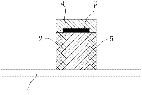
1. A metal circuit structure based on a flexible printed circuit (FPC) comprising: a substrate; a copper layer attached on the substrate; a tin layer formed on the copper layer; an intermediate layer defined between the copper layer and the tin layer, wherein a first surface of the intermediate layer is connected with the copper layer, and a second surface of the intermediate layer is connected with the tin layer, wherein the intermediate layer comprises a first speculum metal layer to form the second surface, wherein the intermediate layer comprises a nickel layer to form the first surface; and two metal layers formed on two sides of the copper layer, wherein the two metal layers are each made of a second speculum metal.