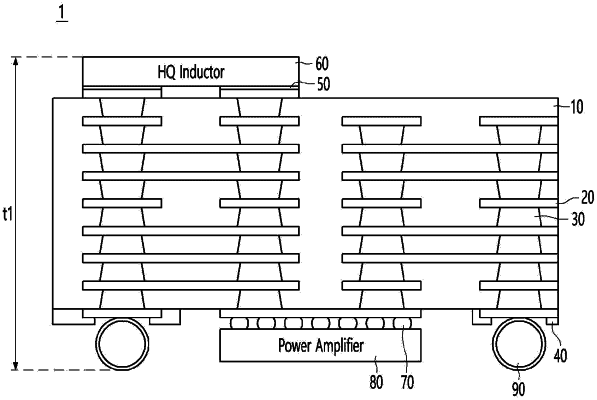
| CPC H05K 1/0296 (2013.01) [H05K 1/115 (2013.01); H05K 2201/09036 (2013.01); H05K 2201/09509 (2013.01); H05K 2201/09854 (2013.01)] | 16 Claims |

|
1. A printed circuit board comprising:
a first insulating layer;
a second insulating layer disposed on the first insulating layer;
a cavity formed in the first insulating layer and the second insulating layer;
a first via electrode disposed in the first insulating layer;
a second via electrode including a portion disposed in the second insulating layer;
an intermediate circuit layer disposed between the first via electrode and the portion of the second via electrode; and
a semiconductor device disposed in the cavity,
wherein the first via electrode overlaps the portion of the second via electrode and the intermediate circuit layer in a vertical direction,
wherein the cavity includes a first side wall having a first slope angle and a second side wall having a second slope angle smaller than the first slope angle, and
wherein the semiconductor device overlaps the portion of the second via electrode, the first side wall of the cavity, and the second side wall of the cavity in a horizontal direction perpendicular to the vertical direction.
|