| CPC H04N 25/709 (2023.01) [H04N 25/78 (2023.01); H04N 25/704 (2023.01); H04N 25/75 (2023.01)] | 21 Claims |

|
1. An imaging device, comprising:
a pixel array including a plurality of pixel circuits arranged in rows and columns;
a plurality of bitlines coupled to the plurality of pixel circuits; and
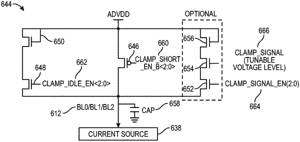
a plurality of clamp circuits coupled to the plurality of bitlines, wherein each one of the plurality of clamp circuits comprises:
a clamp short transistor coupled to a power line and a respective one of the plurality of bitlines of the pixel array, wherein the clamp short transistor is configured to be switched in response to a clamp short enable signal;
a first diode drop device coupled to the power line; and
a clamp idle transistor coupled to the first diode drop device such that the first diode drop device and the clamp idle transistor are coupled between the power line and the respective one of the plurality of bitlines, wherein the clamp idle transistor is configured to be switched in response to a clamp idle enable signal.
|