| CPC H04N 25/47 (2023.01) [H04N 25/77 (2023.01)] | 15 Claims |

|
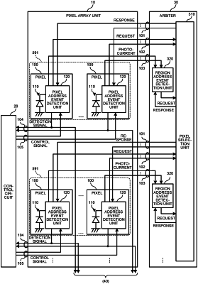
1. An image pickup element comprising:
a plurality of pixels provided with a photoelectric conversion unit that performs photoelectric conversion of incident light;
a pixel address event detection unit that is arranged in each of the plurality of pixels and detects a pixel address event, the pixel address event being an address event of the each of the plurality of pixels and being detected based on a change in a charge amount generated by the photoelectric conversion;
a region address event detection unit that detects a region address event, the region address event being an address event in a predetermined region and being detected based on a change in a charge amount generated by photoelectric conversion in a plurality of pixels included in the predetermined region among the plurality of pixels; and
a pixel selection unit that selects a pixel among the plurality of pixels based on the pixel address event detected and the region address event detected, and causes the pixel selected to output a detection result of the pixel address event.
|