| CPC H04N 23/80 (2023.01) [G06V 20/60 (2022.01); H04N 23/45 (2023.01); G06V 2201/07 (2022.01)] | 10 Claims |

|
1. An imaging device, comprising:
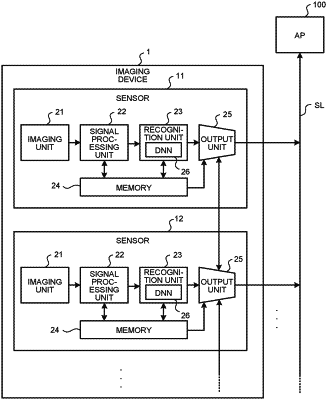
a plurality of image sensors that output detection results to a processing device by sharing one signal line,
wherein at least one of the image sensors includes:
an imaging unit that captures an image to generate image data;
a recognition unit that recognizes a predetermined target object from the image data; and
an output unit that outputs a recognition result of the recognition unit to the processing device in a period that does not overlap with a period in which the detection result of another image sensor is output using the signal line in one frame period in which the imaging unit captures one image.
|